Australian National University Researchers Develop Novel Measurement Tech
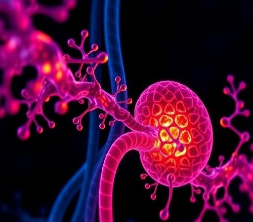
Until recently, multi-material 3D fabrication at nanoscale was the holy grail of nanotechnology and a crucial enabler for the development of new technologies, including photonic, electronic, and biomedical devices. Now, an international team has developed a 3D nanofabrication platform that for the first time realises multi-material fabrication.
This means it is able to make a great variety of materials, including metals, alloys, semiconductors, polymers, ceramics and biomaterials at a record-setting resolution of 20 nanometres, and a light patterning speed of 300 mm3/hour, three orders of magnitude faster than conventional serial fabrication systems that are currently used in the commercial world.
The project, led by Professor Chen Shih-Chi from The Chinese University of Hong Kong (CUHK)’s Department of Mechanical and Automation Engineering, in collaboration with Professor Zhao Yongxin from Carnegie Mellon University (CMU)’s Department of Biological Sciences and Professor Zhao Ni from CUHK’s Department of Electronic Engineering, was recently published in the journal Science, affirming its status as a technological breakthrough, ushering in a new era for nanoscale 3D printing.
Three years ago, Professor Chen and Professor Zhao had a conversation that sparked a collaboration; it aimed to find innovative solutions to long-standing challenges in nano- and micro-fabrication; developing ways to break the limit on material selection and improve the resolution of printable nanodevices to as small as 10 nanometres at a reasonable fabrication rate for practical applications.
Professor Chen is known for inventing the femtosecond projection two-photon lithography system (an ultrafast nano-printing method, reported in the journal Science in 2019), while Professor Zhao’s Biophotonics Lab develops novel techniques to study biological and pathological processes in cells and tissues. In combining their techniques and expertise, the results of their collaboration have opened new doors for the realisation of sophisticated nanodevices.
Professor Chen noted that a major challenge in nanotechnology fabricating complex 3D structures with materials beyond polymers and noble metals. Previously, this had been limited by photo-initiated chemical reactions. Based on the unique surface properties and nanostructures of the femtosecond light sheet-patterned hydrogel identified by the team, a kinetically controlled nano-assembly process was proposed to substitute the conventional photo-reactions.
As the strategy relies on the physical properties of functional materials, such as sizes or hydrophilicity, the limit of material selections can be entirely overcome. Next, by shrinking the patterned gel substrate in acid, we can easily break the diffraction barrier.
Consequently, the team developed a general strategy for fabricating arbitrary 3D nanostructures with a library of materials including metals, metal alloys, 2D materials, oxides, diamond, up-conversion materials, semiconductors, polymers, biomaterials, molecular crystals, and inks.
Their research used hydrogels patterned by femtosecond light sheets as templates. This enabled the direct assembly of materials to form designed nanostructures. By fine-tuning the exposure strategy, the features of the patterned gel and the kinetic effects, the team realised 2D and 3D structures of 20- to 200-nm resolution.
The team fabricated nanodevices, including encrypted optical storage, diffractive optical elements, and microelectrodes, to highlight the precision and the designed functions as well as to demonstrate the promising capabilities of the new method.
The optical storage device set a record for storage density (1.14 petabit/cm3, approximately three orders of magnitude higher than the previous record), and simultaneously set a new record for data-writing speed (84 Mbit/s), owing to the high-speed nature of the femtosecond projection method.
The novel method provides a systematic solution for nanofabrication across different classes of materials and opens further possibilities for the design of sophisticated nanodevices, creating pathways for viable manufacturing of a wide variety of technologies.
Professor Chen further explained that the method be used to make micro- and nanodevices not previously possible as well as make them at high throughput and low cost for practical applications in photonics, health, automobiles and even aerospace.
Looking ahead, the researchers’ goal is to build functional nanodevices with multiple materials, like nanocircuits, nanobiosensors, light-emitting diodes, and lasers, for different applications.