A Conversation with a Researcher and Semiconductor Packaging Expert, Dr. Vinith Bejugam
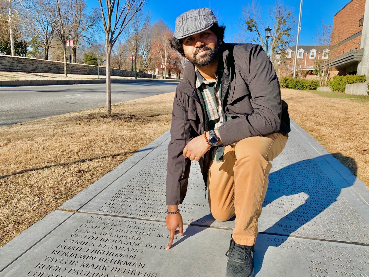

Vinith Bejugam has had an illustrious career pursuing scientific knowledge and developing an understanding of the world around him – and he’s only just getting started. As an avid science-fiction fan, Dr Vinith Bejugam has always been inspired by his curiosity which has led to some impressive collaborations and discoveries.
One only must look at his non-linear mindset and ethics to understand the innate sense of purpose Dr Vinith Bejugam derives from his pursuits, completing a PhD in Chemical Engineering and eventually landing a job at Intel. Dr Bejugam sat down with us and discussed his academic history, his inspiration, and what it is like working at Intel as an R&D Packaging Engineer.
Hello Vinith, thank you for speaking with us! Let’s start with you telling us a little about yourself?
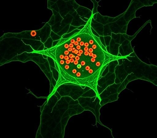
Namaste, I am from Hyderabad, India. After finishing my bachelor’s, I flew to Arkansas for my PhD in Chemical Engineering. My research focused on opto-thermal characterization of plasmon and coupled lattice resonances in gold nanoparticle arrays for applications related to microelectronics, photonics, sensing, and chemical separations. I also worked on research related to electroless plating.
Currently, I am working for Intel as an R&D Packaging Engineer.
What inspired you to pursue a PhD in Chemical engineering? How was your journey?
I am a big sci-fi aficionado. Legendary writer, Michael Crichton’s techno-thrillers had a profound impact on me and incubated my interest in science and technology. His science fiction novels spurred my imagination and I used to have over-the-top notions of becoming a scientist and embark upon an adventurous journey to solve critical world problems.
When I was in high school, I was fascinated with the idea of conducting lab experiments for driving scientific discoveries and creating disruptive technologies as an outcome. I like Pasteur’s Quadrant type of research which aims at seeking fundamental understanding of scientific problems, while also having immediate use for society.
However, I was undergoing immense family / societal pressure in terms of breaking into top-notch engineering institutions in India. I was struggling to keep up with my classmates in terms of grades who were racing ahead by leaps and bounds to get into the IITs and NITs of India. Ironically, I lost interest to become an engineer. I stopped going to school for 6 months. I didn’t want to be part of a race. I just did average work but fortunately I still managed to secure an engineering seat in an institution, which was situated in the outskirts of Hyderabad. Thanks to my dad’s business related to membranes and water technologies, I was motivated to pursue Chemical Engineering. I used to travel 2 hours by bus to my college every morning and 2 hours back in the evening. It went on like this for four years.
During my bachelor’s I was a blogger and once stumbled upon the Nanobiophotonics webpage of my Ph.D. advisor, Dr. Keith Roper, because of whom I developed an interest in Nanotechnology. I wanted to integrate research related to membrane science with Nanotechnology, which motivated me to apply for a PhD degree.
What was your journey while doing your PhD?
When I joined my PhD after completing bachelor’s, and skipping a master’s, I felt like I was not ready and lacked experience in basic research methodologies. Although I am an engineer, I was inclined to think more creatively than analytically. I was rightly branded as a non-linear information processor. But I had the best coach of my life as an advisor. Dr. Roper was an unwavering pillar of support throughout my graduate career. His experience and in-depth knowledge in Chemical Engineering and Nanotechnology has benefitted my work greatly.
My PhD career was like a perfect training exercise in terms of a) critical and analytical thinking, b) conducting rigorous, lengthy, and intricate lab experiments, c) problem-solving, d) becoming more conscientious, e) and learning the art of perseverance. My PhD degree gave me the confidence of a lifetime. I have had wonderful moments where I made cool, serendipitous discoveries. I cannot share or publish all of them, but it was immensely satisfying.
How is it working for Intel?
Intel has a legacy and a great reputation as one of the oldest semiconductor companies in the world. It’s an honour, and a dream to work here. My time at Intel has been very rewarding in terms of work-life balance, research, and various perks that I am entitled to. I am part of a diverse team composed of individuals with highly motivated and professional mindsets.
Managers are not like bosses but rather like leaders here and my colleagues are my source of inspiration. I see no competition but only mutual admiration and interdependency. I am excited about my work here and looking forward to ticking off many important milestones of semiconductor packaging research.
You have an impressive number of publications, an interesting one is “A study about 3D stacking of passive SMD elements for advanced SMT packaging using laser assisted bonding”. What is it about?
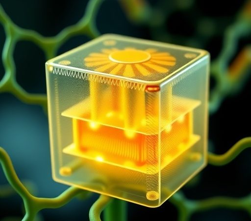
Growing interest in high-performance, compact, and scalable electronic devices or packages which come at competitive prices led to the development of three-dimensional (3D) stacking technologies for juxtaposing various components on top of each other. Think of it as a LEGO game! Heterogeneous integration using 3D stacking involves combining separately manufactured components / chips into a higher-level assembly that could coherently provide an enhanced functionality and improved performance along with offering low power consumption, miniaturization, high reliability, and faster speeds.
Now that we established the context, this paper was a collaborative effort with colleagues (Matthias Fettke et al) from my previous job at Pac Tech—Packaging Technologies Inc., Santa Clara. This work demonstrated a laser-assisted bonding (LAB) method for 3D stacking of capacitors. This work highlights advantages of LAB such as its non-invasive nature, rapid cycle time, and highly controlled output for obtaining defect-free solder interconnections. Also, LAB’s performance was compared with conventional oven reflow processes.
Overall, this paper demonstrated a feasible, facile, and non-destructive method for chip stacking that precludes any deleterious effects of thermal, physio-chemical, and mechanical stresses in the package. Additionally, any diffusion effects at the interfaces between solder and pad could be minimized.
What is next for Vinith Bejugam?
I think I am at another inflection point in my career. Although I learned a lot, I still feel dumb every day, and my learnings won’t stop ever in this lifetime. My love for science and fiction will probably lead me in a path where I would aim to spread positive energy and share my learnings with future generations. Life is full of surprises and opportunities. You can also create your own opportunities!
“Every next level of your life demands a different you” – Leonardo Di Caprio
Thank you Dr.Bejugam for your time!
You can follow up with Dr. Vinith Bejugam at https://www.linkedin.com/in/vinithbejugam
