| Nov 15, 2022 |
|
|
|
(Nanowerk Spotlight) The discovery of magnetism in two-dimensional (2D) ultrathin crystals opens up opportunities to explore new physics and to develop next-generation spintronic devices. However, 2D magnetic semiconductors with Curie temperatures higher than room temperature have rarely been reported.
|
|
Ferrites with strongly correlated d-orbital electrons may be alternative candidates offering 2D high-temperature magnetic ordering. This prospect is, however, hindered by their inherent three-dimensional bonded nature.
|
|
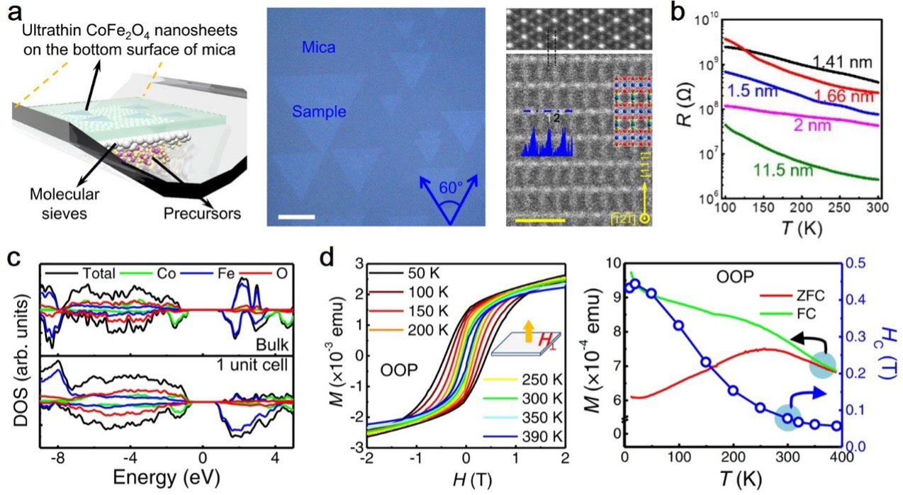
“In this context, we show that high-quality, nonlayered cobalt ferrite nanosheets as thin as a single unit cell can be synthesized via van der Waals epitaxy,” Dr. Ruiqing Cheng from the School of Physics and Technology, Wuhan University, in Wuhan, tells Nanowerk. “The introduction of van der Waals substrates and confined conditions enables the van der Waals interactions between overlayers and substrates rather than the misfit energy to govern the crystal growth during the chemical vapor deposition process. This strategy is also applicable to the synthesis of other spinel-type nanosheets.”
|
|
The researchers have published their findings in Nature Communications (“Ultrathin ferrite nanosheets for room-temperature two-dimensional magnetic semiconductors”).
|
 |
| Figure 1. Van der Waals epitaxial growth of ultrathin cobalt ferrite nanosheets, as well as their semiconducting and magnetic properties. (Image courtesy of the researchers) (click on image to enlarge)
|
|
In this work, the hard magnetic behavior of cobalt ferrite nanosheets is demonstrated by means of vibrating sample magnetometry, magnetic force microscopy and magneto-optical Kerr effect measurements, which shows high Curie temperature above 390 K and strong dimensionality effect. Besides, the researchers found no apparent change in magnetic properties after exposure to ambient conditions for over a month.
|
|
The ultrathin thickness in the vertical direction could make the control of magnetic order through electrostatic gating, heterostructuring and strain more efficient compared with 1D or bulk architecture. Theoretical modelling shows that the lack of atoms on the other side of the surface would make the magnetic configuration deviate from the Néel-type spin alignment. As a result, the spin polarization is enhanced.
|
|
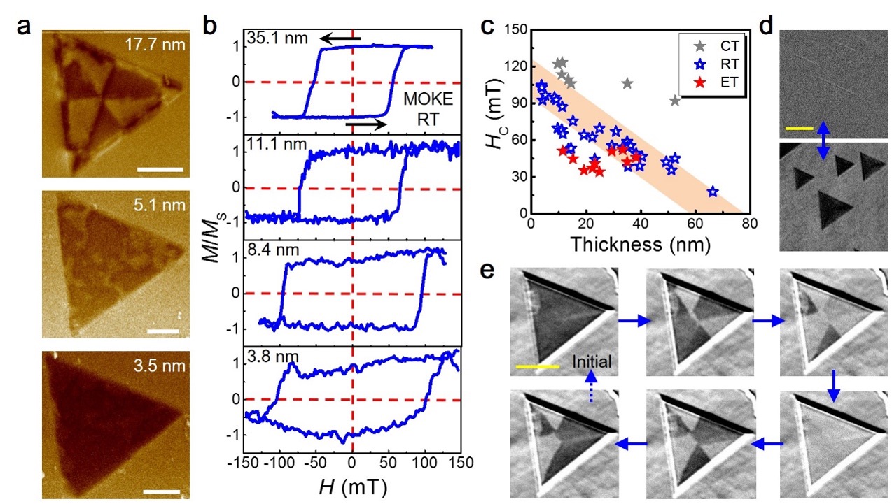
For the relatively thick nanosheet, its domain structures are partitioned into multiple uniform domains with anti-parallel magnetization. The square hysteresis loops clearly demonstrate the out-of-plane magnetic anisotropy. As the sample thickness decreases, the reduction in the magnetostatic energy cannot compensate for the increase in the energy of domain walls, the magnetic structure shows a transition from multiple domain to single domain.
|
|
The decrease of coercive force from 104.6 mT to 18.0 mT is observed with the increased nanosheet thickness from 3.7 nm to 66.3 nm at room temperature.
|
 |
| Figure 2. Thickness-dependent magnetic properties of cobalt ferrite nanosheets. (Image courtesy of the researchers) (click on image to enlarge)
|
|
The realization of room-temperature 2D magnetic semiconductors could greatly enrich the available 2D candidates and extend their application prospects. The authors also show the potential of the van der Waals epitaxy method in wafer-scale ultrathin ferrite film and demonstrate that it is feasible to increase the ferrite coverage on the substrate by adjusting the growth parameters. This is the prerequisite for mass production and will be the next breakthrough in this area.
|
|
Provided by the School of Physics and Technology, Wuhan University
|
|
|
