Canon on cusp of nanoimprint chip-making revolution

Canon is moving ahead with a plan to build a new factory in Japan to double the production of its semiconductor lithography equipment.
The planned facility will produce both the standard KrF and i-line machines that constitute the bulk of the division’s sales and the nanoimprint tools that Canon hopes will open a new era in semiconductor manufacturing.
Addressing investors after the announcement of third-quarter results in late October, Canon’s management referred to “our leading-edge nanoimprint lithography equipment.”
Indeed, Canon’s lithography gear is leading edge in the nanoimprint world. But is it a threat to ASML’s monopoly on extreme ultraviolet (EUV) photo-lithography equipment, as some have suggested?
Canon’s new factory will be built in Utsunomiya, north of Tokyo, at an estimated cost of over 50 billion yen (US$357 million) including equipment. Operations are scheduled to begin in 2025, when Kioxia reportedly plans to start using nanoimprint lithography in mass production of its NAND flash memory.
Kioxia, formerly a division of Toshiba and now an affiliate, makes NAND flash memory chips in a joint venture with Western Digital. It is the second largest producer after Samsung Electronics with about 30% of the global market. NAND flash memory chips are used to store information in solid state drives, USB flash drives, SD cards, digital cameras and cell phones.
Toshiba/Kioxia, Canon and photomask maker Dai Nippon Printing have been working on nanoimprint technology for several years. Canon entered the nanoimprint business in 2014 through its acquisition of Molecular Imprints, a spinout from the University of Texas in Austin.
Now known as Canon Nanotechnologies, the company has secured more than 170 patents covering imprint tools, materials, masks, process technology and imprint-specific device designs.
Other producers of nanotech lithography equipment include Electronic Visions Group (EVG), SUSS MicroTec and Obducat, all of which are European.
Dai Nippon Printing established a commercial production system for nanoimprint templates in 2015. Toshiba announced plans to use the technology to make NAND flash memory in 2016.


Canon originally hoped to begin mass production by 2019 but that superfast timeline proved unrealistic. Nanoimprint equipment has been installed at Kioxia’s Yokkaichi NAND fabrication site but is not yet used in mass production.
In contrast to photo-lithography, in which light from a scanner passes through a photomask to transfer circuit patterns to a wafer coated with a photo-sensitive resist, nanoimprint lithography is a miniature mold and stamping process.
However, there are reportedly still problems with overlay, throughput and defects, including particles created by the physical contact inherent in the process.
In theory, nanoimprint lithography could offer a 90% reduction in power consumption, a 40% reduction in overall processing costs, and equipment priced at a fraction of ASML’s EUV scanners. In practice, it is not yet clear when it might become an integral part of Kioxia’s NAND flash production process.
Nanoimprint lithography is not new. It was invented by Japanese researcher Susumu Fujimori, who patented his UV nanoimprint lithography process in 1979 while working at Nippon Telegraph and Telephone Public Corporation.
In the mid-1990s, the technology was brought to attention in the US by Stephen Chou, Peter Krauss and Preston Renstrom of the NanoStructure Laboratory of the Department of Electrical Engineering at the University of Minnesota. Molecular Imprints was founded in 2001. Dai Nippon Printing began work on the technology in 2003.
The American origins of Canon Nanotechnologies will likely bring nanoimprint lithography manufactured by Canon under US government restrictions on exports to China – just as the use of light sources from San Diego-based Cymer allowed the US to ban the sale of Netherlands-based ASML’s EUV lithography equipment to customers in China.
Canon’s KrF and i-line lithography equipment, on the other hand, is previous generation, not essential to the production of leading-edge semiconductors and thus not subject to US sanctions.
It is a cash cow for Canon and helps China boost production of less sophisticated semiconductor devices that would otherwise have to be imported. When Canon’s new factory comes online, a substantial amount of its output will likely be shipped to China.
Meanwhile, Toppan Printing, Japan’s other large producer of IC photomasks, has tied up with EVG to promote the use of nanoimprint lithography as a high-volume manufacturing technology for the photonics industry.
This is no accident: Toppan and Dai Nippon Printing are competitors and the processes and materials used to produce photomasks and nanoimprint templates are similar.
Potential products include waveguides, metalenses (flat lenses etched on silicon) and other optical components. Applications include virtual reality headsets, smartphone and vehicle sensors, and medical imaging.
EVG is a supplier of equipment used in the manufacture of Micro Electrical Mechanical Systems (MEMS), compound and power semiconductors, optical components and other nanoscale devices.
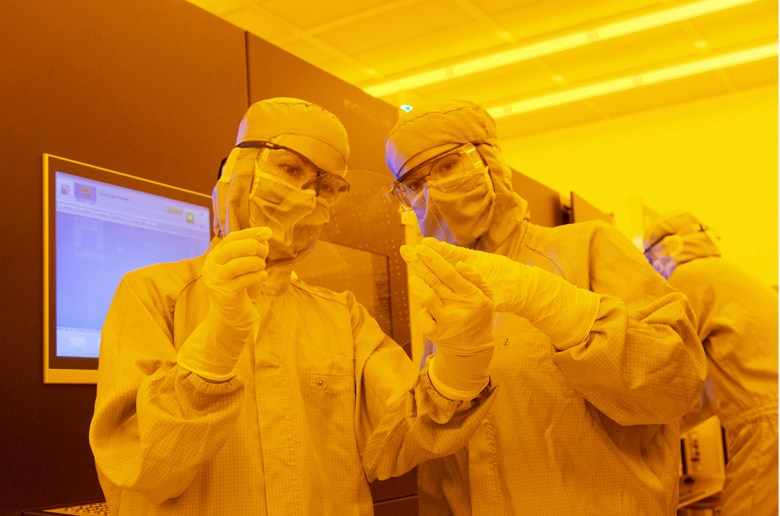

Its products include lithography, bonding, thin-wafer processing, photoresist coating, cleaning, metrology and inspection systems. It began high-volume production of nanoimprint lithography systems in 2015. Headquartered in Austria, it has subsidiaries in the US, Japan, South Korea, China and Taiwan.
In September, EVG and Toppan announced plans to sell nanoimprint lithography development kits combining templates from Toppan with equipment and process development services from EVG.
The two companies regard nanoimprint lithography as a proven, cost-effective alternative to photolithography. Their customers will soon provide feedback on whether that’s the case.
Follow this writer on Twitter: @ScottFo83517667


