| Jan 09, 2023 |
|
|
|
(Nanowerk Spotlight) The Internet of Things (IoT) is a system of interconnected physical objects equipped with sensors, processors, and other technologies that allow for the exchange of relevant data over the internet.
|
|
In 1999, British technologist Kevin Ashton coined the term Internet of Things to define a network that not only connects people, but also the objects around them. According to Ashton, “the IoT network integrates the interconnectedness of human culture – our ‘things’ – with the interconnectedness of our digital information system – the internet.”
|
|
The number of IoT devices is expected to reach 75 billion by 2025, generating potentially hundreds of zettabytes of data. This growth is enabled by technologies such as cloud computing and big data analytics, as well as communication protocols including Bluetooth, Wi-Fi, ZigBee, NFC, LPWA, and 5G.
|
 |
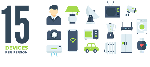
| According to forecasts, the number of IoT connected devices will grow dramatically to 75 billion in 2025 and a staggering 125 billion by 2030. At that point, there will be almost 15 things connected to the Internet for each human on earth. (Source: reply.com)
|
|
As billions of ‘dumb’ inanimate objects have become ‘smart’ (i.e., connected), and billions more are added every year, the IoT is now at work all around us. RFID tags track produce from harvest to store shelf; GPS systems guide cars, ships and planes to their destinations; streetlights dim when there is no car nearby; smart room controls turn off heat, air conditioning and lights when rooms are unoccupied.
|
|
Industries and governments now use IoT to understand consumer needs in real time; become more responsive; improve production processes and entire factory efficiencies; transform communities into smart cities.
|
Nanotechnology has the potential to impact and improve several key components of the IoT
|
|
Key components that are essential to the functioning of the Internet of Things include sensors and devices, network connectivity, data storage and processing, user interfaces, and security. Many aspects of these elements can be enhanced by nanotechnologies. These include:
|
|
Sensors and devices: These are the “things” in the Internet of Things, and they are equipped with sensors that can collect data about their environment, such as temperature, humidity, location, and motion.
|
|
Nanomaterials can be used to create smaller, more sensitive sensors that are capable of detecting a wide range of parameters, including temperature, humidity, pressure, and chemical composition. Nanosensors use a variety of nanomaterials to monitor physical, chemical, and biological phenomena, and can have advantages in terms of sensitivity, response time, and power consumption.
|
|
For example, carbon nanotubes and graphene have been used to create highly sensitive sensors for detecting gases and pollutants.
|
|
One great example of these new types of sensors and how they can be used in novel ways is a ‘tooth tattoo’ sensor that may help dentists assess patients’ oral health:
|
 |
| The sensor (A), attached to a tooth (B) and activated by radio signals (C), binds with certain bacteria (D). (Illustration: Manu Mannoor)
|
|
The sensor is relatively simple in its construction and made up of just three layers: a sheet of thin gold foil electrodes, an atom-thick layer of graphene, and a layer of specially engineered peptides, chemical structures that “sense” bacteria by binding to parts of their cell membranes.
|
|
Powering these devices requires energy and researchers are working on various ways of doing that. For instance, the size of the single solar cell used in IoT applications is much smaller, and in combination with the lower power input available in low-light indoor settings as well as the emission spectra of light sources other than the sun, renders the need for high conversion efficiency paramount.
|
|
A recent progress report compares emerging indoor photovoltaic technologies with alternative energy harvesters (piezoelectric, triboelectric, thermoelectric, and ambient RF) and provides a great overview of this field (“Emerging Indoor Photovoltaic Technologies for Sustainable Internet of Things”).
|
|
As another recent review explains and addresses in great detail (Advanced Functional Materials, “Advances in Organic and Perovskite Photovoltaics Enabling a Greener Internet of Things”), the requirements that solar cells should satisfy to power IoT devices are quite different to the ones usually deemed necessary for application in outdoor-placed solar panels.
|
|
Network connectivity: In order for the sensors and devices to communicate with each other and with the wider internet, they need to be connected to a network. This could be a local area network (LAN), a wide area network (WAN) such as the internet, or a combination of both.
|
|
Nanostructures can be used to improve network connectivity. For instance, nanomaterials such as graphene, quantum dots and silver nanowires can be used to create smaller, more efficient antennas and other components that are essential for wireless communication. These materials have high conductivity and can transmit signals over long distances with minimal loss.
|
|
Nanoantennas, often made from graphene, can be used for wireless communication in the terahertz frequency band and can be consolidated with nanosensors using carbon nanotubes.
|
|
In addition, nanostructures such as nanoparticles and nanofilms can be used to create more efficient and robust wireless communication systems, such as those used in satellite and 5G networks.
|
|
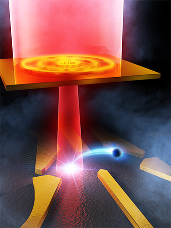
Well-established nanophotonics technologies will enable the secure quantum communication and information networks that are required by the IoT. For instance, a recently demonstrated nanoantenna will help bring quantum information networks closer to practical use. Here, researchers have substantially enhanced photon-to-electron conversion through a metal nanostructure, which is an important step forward in the development of advanced technologies for sharing and processing data.
|
 |
| Conceptual illustration of efficient illumination of photons to semiconductor lateral quantum dots, by using a surface plasmon antenna and excitation of electrons in the quantum dots. (Image: Oiwa lab, Osaka University)
|
|
Data storage and processing: The data collected by the sensors and devices needs to be stored somewhere, and often needs to be processed in order to be useful. This is typically done using servers and cloud computing resources.
|
|
Nanostructures such as nanoparticles and nanofilms can be used to create denser, more efficient storage media, such as hard drives and memory chips. For example, researchers have used nanoparticles to create high-density data storage media with a capacity that is several orders of magnitude higher than current hard drives.
|
|
In addition, nanoelectronics could be used to create faster, more powerful processors and other computing components. For example, researchers are exploring the use of quantum dot technology to create ultra-fast, low-power processors.
|
|
Avoiding traditional silicon chips and instead using a fabrication technique called transfer printing, researchers have developed nanoelectronics stickers specifically for the use with IoT devices. These tiny, thin-film electronic circuits are peelable from a surface. The technique not only eliminates several manufacturing steps and the associated costs, but also allows any object to sense its environment or be controlled through the application of a high-tech sticker. Watch the video:
|
|
[embedded content]
|
|
User interfaces: In order for people to interact with the IoT system, there needs to be some kind of user interface, such as a smartphone app or a web-based dashboard.
|
|
Nanostructures can be used to create smaller, more portable devices such as smartphones and tablets. For example, researchers are exploring the use of flexible nanomaterials such as graphene and silver nanowires to create bendable and foldable displays.
|
|
Smart fabrics could be used to monitor vital signs and provide real-time information to users, and could be used for industrial purposes to ensure worker safety.
|
|
In addition, nanostructures can be used to improve the performance and efficiency of displays and other components, such as touchscreens, cameras, and speakers. For example, nanoparticles can be used to create brighter and more efficient displays, and nanofibers can be used to create more powerful speakers.
|
|
Security: Ensuring the security of an IoT system is critical, as it involves sensitive data and the potential for malicious actors to compromise the system.
|
|
Nanomaterials can be used to create more secure, anti-counterfeiting authentication systems, such as biometric sensors and nanoscale security features. For example, researchers are exploring the use of carbon nanotubes for physically unclonable functions.
|
|
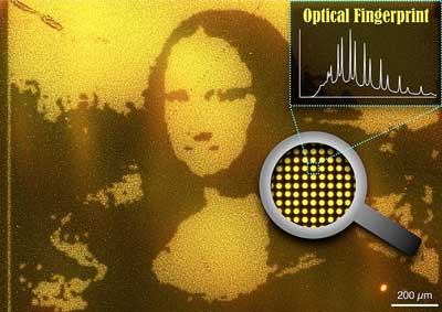
Another example is an optical microresonator array with unreplicable spectral fingerprints to create optical patterns that cannot be duplicated. The researchers used their technology to create a millimeter-size approximation of the Mona Lisa (see image below). This approximation contains a unique, embedded fluorescence fingerprint that cannot be duplicated.
|
 |
| Researchers from the University of Tsukuba create millimeter-size chips with unique color patterns that cannot be forged.
|
|
In addition, nanostructures can be used to create more robust and resilient network infrastructure, which can help to prevent attacks and improve the overall security of the IoT system. For example, researchers are exploring the use of nanomaterials to create more secure and efficient encryption systems, and to create networks that are more resistant to interference and jamming.
|
|
In terms of terminology, some argue that the Internet of Things has given rise to the concept of the Internet of Nano Things (IoNT), which is a communication network paradigm based on nanotechnology that enables the interconnection of nanoscale devices through existing networks.
|
|
In other words: the IoNT isn’t that different from the IoT – except that is connects nanoscale devices, objects and even organisms. For the purpose of this article, we stick just to the IoT.
|
Specific examples of how nanotechnology is being used to enhance the IoT
|
|
Longer-lasting batteries: Nanoparticles can be used to create more efficient and longer-lasting batteries for IoT devices. For example, mechanical engineers at the University of Maryland have demonstrated that using nanotechnology in batteries will improve battery performance. This could lead to IoT devices with much longer battery life, reducing the need for frequent charging.
|
|
More sensitive and accurate sensors: Nanosensors are incredibly small sensors that can detect a wide range of physical, chemical, and biological parameters. They can be used to improve the sensitivity and accuracy of IoT devices, such as wearable fitness trackers or environmental monitoring systems. For example, researchers at the University of California, Berkeley have developed a nanosensor that can detect trace amounts of toxic gases and turn your smartphone into a smart gas sensor.
|
|
Self-powered systems: Self-powered nanotechnology based on piezoelectric nanogenerators aims at powering nanodevices and nanosystems using the energy harvested from the environment in which these systems are suppose to operate. This offers a completely new approach for harvesting mechanical energy using organic and inorganic materials. These nanogenerators could be used to power small, lightweight IoT devices, such as wearable sensors, without the need for external batteries.
|
|
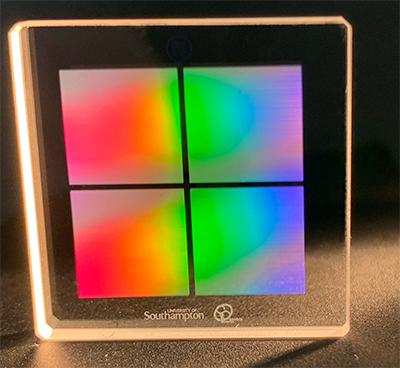
Enhanced data storage: Nanostructures can also be used to improve data storage in IoT devices. For example, researchers at the University of Southampton have developed a fast and energy-efficient laser-writing method for producing high-density nanostructures in silica glass. These tiny structures can be used for long-term five-dimensional optical data storage that is more than 10,000 times denser than Blue-Ray optical disc storage technology. |
 |
| Researchers developed a new fast and energy-efficient laser-writing method for producing nanostructures in silica glass. They used the method to record 6 GB data in a one-inch silica glass sample. The four squares pictured each measure just 8.8 X 8.8 mm. They also used the laser-writing method to write the university logo and mark on the glass. (Image: Yuhao Lei and Peter G. Kazansky, University of Southampton)
|
|
Improved wireless communication: Single-layer molybdenum disulfide (MoS2) can be used to improve wireless communication in IoT devices by increasing the speed and range of data transmission. For example, researchers at the University of Texas at Austin have developed flexible radio frequency (RF) transistors operating at GHz performance, which very promising for the design of low-power and high-frequency flexible RF nanoelectronics systems.
|
|
Another example is a tunable, graphene-based device that could significantly increase the speed and efficiency of wireless communication systems such as the IoT. The device, which is only several hundred micrometers (around 0.05 cm) long and wide, can be stiff or flexible, is easily miniaturized, and uses very little energy. In addition to improving the flow of data between connected devices, it could extend battery life and lead to ever more compact devices. In its flexible state, it could be easily used in sensors placed in clothes or directly on the human body.
|
|
Increased durability: Nanoparticles can be used to make IoT devices more durable and resistant to wear and tear. For example, researchers at Osaka University have developed cohesive circuit protection for wearable electronics using self-healing cellulose nanofibers.
|
|
Improved data security: Quantum Cryptography is one emerging security technology that offers radically new protection measures for communication systems. At the heart of any quantum system is the most basic building block, the quantum bit or qbit, which carries the quantum information that can be transferred and processed (this is the quantum analogue of the bit used in current information systems). The most promising carrier qbit for ultimately fast, long distance quantum information transfer is the photon, the quantum unit of light. Already, researchers have demonstrated an efficient and compact single photon source that can operate on a chip at ambient temperatures. Using quantum dots, the scientists developed a method in which a single nanocrystal can be accurately positioned on top of a specially designed and carefully fabricated nano-antenna. Such highly directional single photon source could lead to a significant progress in producing compact, cheap, and efficient sources of quantum information bits for future quantum technological applications
|
|
Advanced medical devices: Nanomaterials and -structures can be used to create advanced medical devices for use in the IoT, such as smart pills that can monitor and diagnose medical conditions from inside the body. For example, engineering researchers at the University of California, San Diego, have developed a battery-free, pill-shaped ingestible biosensing system designed to provide continuous monitoring in the intestinal environment. It gives scientists the ability to monitor gut metabolites in real time.
|
 |
| The self-powered ingestible sensor system designed to monitor metabolites in the small intestine over time. (Image: David Ballot, Jacobs School of Engineering, UC San Diego)
|
|
Enhanced renewable energy: Nanotechnology can be used to improve the efficiency of renewable energy technologies, such as solar panels, for use in the IoT. For example, materials scientists at the University of California, Los Angeles, have developed a highly efficient thin-film solar cell that generates more energy from sunlight than typical solar panels, thanks to its double-layer design. The cell’s copper, indium, gallium and selenide (CIGS) base layer, which is about 2 microns thick, absorbs sunlight and generates energy on its own, but adding a 1 micron-thick perovskite layer improves its efficiency – much like how adding a turbocharger to a car engine can improve its performance. The two layers are joined by a nanoscale interface that the researchers designed; the interface helps give the device higher voltage, which increases the amount of power it can export. (For more on this read: “Perovskite photovoltaics for a greener Internet-of-Things“)
|
Conclusion
|
|
In conclusion, the combination of nanotechnology and the Internet of Things has the potential to bring significant benefits and improvements to a wide range of applications. Nanotechnology can enhance the performance and capabilities of IoT devices by enabling the creation of smaller, more efficient, and more versatile sensors, antennas, and processors. These improvements can lead to greater accuracy, energy efficiency, and versatility in a variety of applications, including healthcare, industrial monitoring, and environmental sensing.
|
|
However, there are also challenges and limitations to using nanotechnology in the IoT, including the cost of production, communication and processing limitations, and susceptibility to physical damage and interference. To overcome these challenges, it will be important to continue researching and developing strategies for addressing these issues, as well as exploring new IoT-relevant applications and technologies that can take advantage of the unique capabilities of nanotechnology.
|
|
Overall, the intersection of nanotechnology and the IoT holds great promise for the future, and it will be interesting to see how these two technologies continue to evolve and intersect in the coming years.
|
By
Michael
Berger
–
Michael is author of three books by the Royal Society of Chemistry:
Nano-Society: Pushing the Boundaries of Technology,
Nanotechnology: The Future is Tiny, and
Nanoengineering: The Skills and Tools Making Technology Invisible
Copyright ©
Nanowerk
|
|
|
