New SIA Map Highlights Broad U.S. Semiconductor Ecosystem
Reading time ( words)
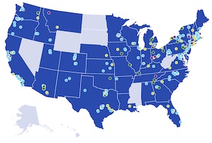
The semiconductor ecosystem in the United States is broad and diverse, as illustrated by SIA’s new U.S. Semiconductor Ecosystem Map, a first-of-its-kind tool that allows users to explore industry activities across the country, including nearly 500 locations in 42 states. This expansive ecosystem is comprised of semiconductor manufacturing, chip design, intellectual property and chip design software providers, semiconductor materials and manufacturing equipment, and research and development, including university R&D partners of the Semiconductor Research Corporation (SRC) and the National Nanotechnology Coordinated Infrastructure (NNCI).
Of particular note, the U.S. Semiconductor Ecosystem Map highlights announced company investments for new and expansion semiconductor ecosystem projects. These projects cover a range of activities needed to bolster the U.S. chip ecosystem, including new, expanded, or upgraded fabs in various semiconductor segments (e.g., advanced logic, memory, analog, and legacy chips), semiconductor equipment facilities, and facilities to produce key materials used in the chip manufacturing process. From the time the CHIPS Act was introduced in the Spring of 2020 through the months following its enactment in August 2022, companies in the semiconductor ecosystem announced dozens of projects to increase manufacturing capacity in the U.S. As of March 2023, some highlights of announcements spurred by the CHIPS Act include:
- Over $210 billion in new private investments announced across 19 states to increase domestic manufacturing capacity
- Over 50 new semiconductor ecosystem projects announced across the U.S., including the construction of new fabs, expansions of existing sites, and facilities that supply the materials and equipment used in chip manufacturing
- 44,000 new high-quality jobs announced in the semiconductor ecosystem as part of the new projects, which will support many more jobs throughout the broader U.S. economy
As the CHIPS Act incentives and R&D programs continue to be implemented, SIA’s U.S. Semiconductor Ecosystem Map will be updated to reflect the ever-growing domestic semiconductor footprint.
Share
Suggested Items
10/22/2019 |
University of Illinois
As wearable sensors become more prevalent, the need for a material resistant to damage from the stress and strains of the human body’s natural movement becomes ever more crucial. To that end, researchers at the University of Illinois at Urbana-Champaign have developed a method of adopting kirigami architectures to help materials become more strain tolerant and more adaptable to movement.
05/13/2019 |
Rice University
Mixing two brittle materials to make something flexible defies common sense, but Rice University scientists have done just that to make a novel dielectric. Dielectrics are the polarized insulators in batteries and other devices that separate positive and negative electrodes. Without them, there are no electronic devices.
06/05/2017 |
DARPA
The Department of Defense’s proposed FY 2018 budget includes a $75 million allocation for DARPA in support of a new, public-private “electronics resurgence” initiative. The initiative seeks to undergird a new era of electronics in which advances in performance will be catalyzed not just by continued component miniaturization but also by radically new microsystem materials, designs, and architectures.